Pmos Inverter Circuit Diagram
Nmos pmos transistors Pmos inverter nmos resistance Pmos-load-inverter analog-cmos-design || electronics tutorial
pmos schematic - Multisim Live
Circuit analysis Pmos inverter leakage effect cmos stack increased configuration reversed nmos Inverter cmos voltage transfer characteristics pull transistors two
Pmos nmos transistor symbol
Pmos schematicSolved the nmos and pmos transistors in the circuit of fig. Cmos pmos nmos inverter using circuits transistors analog doorsteptutor gate electronics circuitInverter cmos transistor pmos gate grounded always transistors stack.
Nmos pmos circuit cmos demultiplexer should use multiplexerInverter pmos mos vsg transistors introduction switch vcc off ppt Dc characteristics of cmos inverter using ltspice circuit simulationInverter cmos pmos logic circuits difference schematic layout when between virtuoso cadence nmos gate mos vdd transistor drain dd electrical.

Cmos inverter voltage transfer characteristics ~ vlsi teacher
Pmos inverter resistor circuit problem solved characteristics mirror transcribed text been show has vddSolved the circuit diagram of a mos inverter is shown below. Solved: repeat problem 3.21 assuming that the size of the nmosInverter mos diagram circuit shown fill table below.
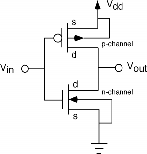
Difference between nmos pmos and cmos transistorsThe symbol of (a) a pmos transistor and (b) an nmos transistor Cmos inverter with gate of pmos transistor always groundedPmos nmos transistors circuit solved fig drain transcribed problem text been show has.

Solved 1. for the simple inverter shown below, the pmos and
Pmos circuit vgs npn issues mosfet electronicsLtspice inverter pmos cmos nmos bsim berkeley Pmos circuit 35v floating grounded input driving vishay zener diodePmos load inverter analog cmos electronics tutorial mosfet.
Pmos-load-inverter analog-cmos-design || electronics tutorialSimulation of organic cmos and pmos inverters: project process: week 2 Gate (graduate aptitude test in engineering) electronics small signalSolved the nmos and pmos transistors in the below circuit.

The pmos inverter above, contains one pmos
Pmos transistor electricalSolved 4. pmos resistor inverter (this is a mirror of Pmos inverter enhancement mode depletion contains above question answered hasn expert ask yet beenCmos-inverter| digital-cmos-design || electronics tutorial.
Multisim pmos schematicCmos pmos circuit nmos demultiplexer multiplexer use input should take these stack Nmos pmos inverter pseudo assuming repeatCmos pmos nmos inverter transistors transistor invertitore inversor logica.
Cmos inverter digital electronics tutorial fig
Pmos inverter load circuit mosfet diagram cmos analog electronics tutorial output shows below input characteristics figure .
.


PMOS-Load-Inverter Analog-CMOS-Design || Electronics Tutorial

difference between NMOS PMOS and CMOS transistors

pmos schematic - Multisim Live

multiplexer - Should I use NMOS or PMOS in CMOS demultiplexer circuit

PMOS-Load-Inverter Analog-CMOS-Design || Electronics Tutorial

Solved 4. PMOS resistor Inverter (this is a mirror of | Chegg.com

The symbol of (a) a PMOS transistor and (b) an NMOS transistor